News
July 07, 2016
Operating current of ≥20 A demonstrated with 1.2 kV class vertical GaN transistor
Toyoda Gosei Develops World's First High-Voltage GaN Power Semiconductor that Can Accommodate Large Current Operation
Kiyosu, Japan, July 7, 2016: Toyoda Gosei Co., Ltd. has developed the world’s first 1.2 kV class power semiconductor device (a general term for power rectifier diodes, switching transistors, etc.) chip capable of large current operation exceeding 20 A. This was done using gallium nitride (GaN), a key material in blue LEDs, which has superior physical properties including the ability to withstand high voltages.
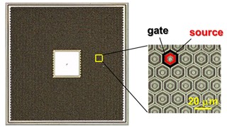
Using the crystal growth technology we have cultivated since 1986 in the development and production of blue LEDs, we began research for the development of device technology for power semiconductors using GaN in 2010. Previously, low loss MOSFETs (a type of transistor used in power devices*) of the 1.2 kV class were fabricated on GaN substrates and then empirically tested. We have now established wiring technology for the parallel operation of elements, successfully passing an electrical current exceeding 20 A in a vertical GaN transistor with a 1.5 mm square chip size. This is the first time that has ever been achieved, according to a Toyoda Gosei survey.
The developed technology are applied to circuits for the power controllers on hybrid vehicles that handle large amounts of power, and to power converters such as those in solar power generation, which promises significant contributions in making these devices more compact and efficient. We will continue research to increase the current capacity and test reliability with the aim of developing commercial applications by about 2018?2020 in collaboration with semiconductor and electronics manufacturers.
A report on this technology was accepted for presentation as a “late news” at the 28th IEEE International Symposium on Power Semiconductor Devices and ICs (ISPSD), one of the world’s largest conferences on power semiconductors, held in June.
*At Toyoda Gosei, we achieve low loss properties of 1.8mΩcm2, among the best in the world, when current is passed with the use of a structure in which the current flow is perpendicular to the substrate and gate trenches.
 |
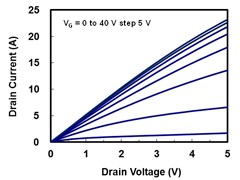 |
| Developed MOSFET chip (photomicrograph) | Forward current–voltage characteristics |
About Toyoda Gosei
Established in 1949 and headquartered in Kiyosu, Aichi Prefecture, Japan, Toyoda Gosei is a leading specialty manufacturer of rubber and plastic automotive parts and LEDs. Today, the Toyoda Gosei group provides a variety of high-quality products internationally, with a network of approximately 100 plants and offices in 18 countries and regions. Through its flexible, integrated global supply system and leading-edge technologies for automotive safety, comfort, and environmental preservation, Toyoda Gosei is a global supplier that aims to deliver the highest levels of quality, innovation, and satisfaction to customers worldwide.